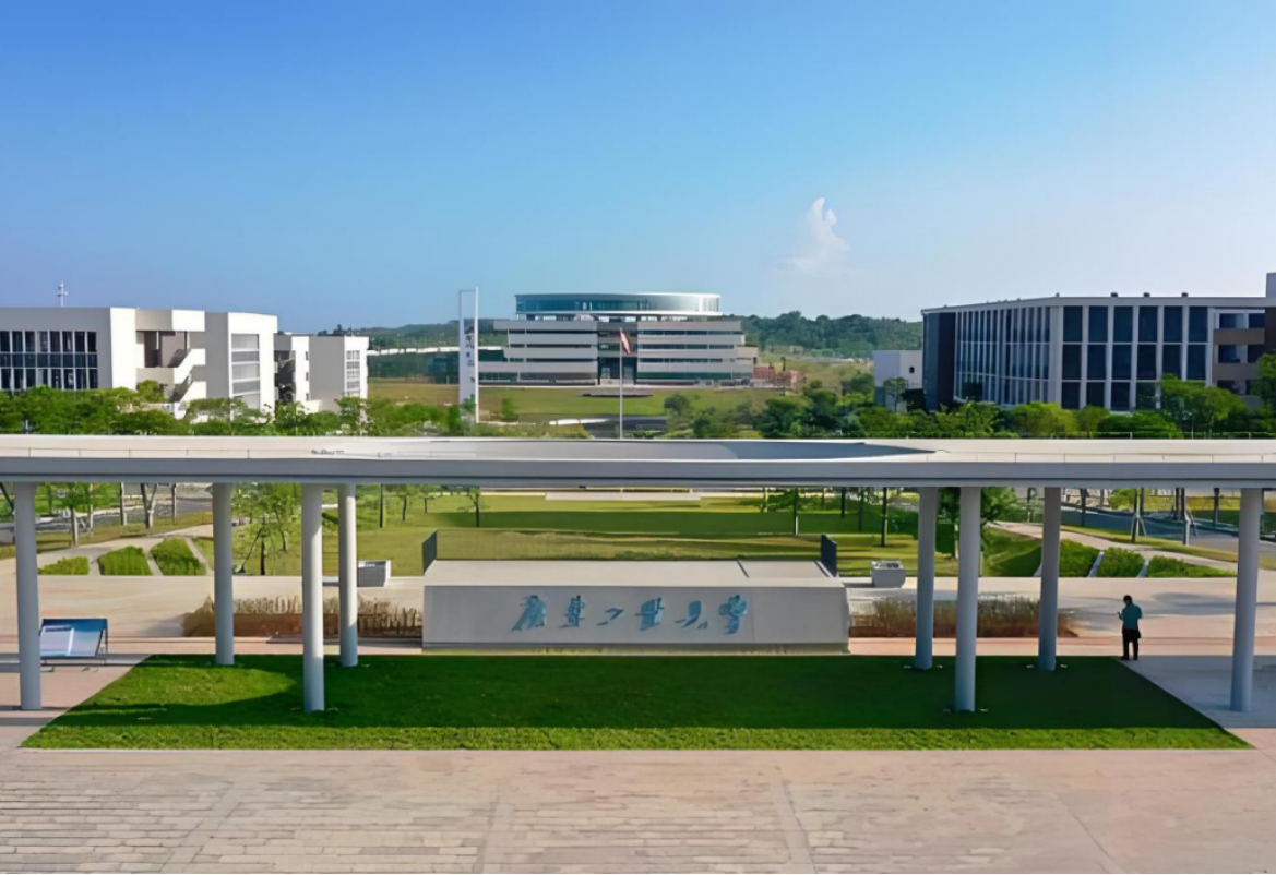
Project: Guangdong University of Technology Semiconductor Micro/Nano Processing R&D and Service Platform Engineering
Location:Guangzhou, Guangdong
Time:2024-2025
Service scope:Cleanroom, special gas system, and secondary distribution engineering.
Main features:Expected to have full process manufacturing capabilities for silicon based on 6-inch wafers, capable of preparing various customized semiconductor thin film materials and devices, CMOS devices and circuits, etc., to meet the needs of micro nano processing research and development and service platforms in the field of integrated circuits.
Confidentiality NoticeThis case involves the client's trade secrets, and it is strictly prohibited to reprint or quote them in any form to the outside world. Violators will be held accountable in accordance with the law.